RFSoC Concept
The RFSoC concept does just that by integrating the multi giga sample ADCs and DACs within the same silicon as the SoC, which contains the processing system and programmable logic. This offers a much tighter integrated solution providing the potential for both reduced footprint and power dissipation, while providing a direct sampling RF solution for 5G applications. Integration of ADC and DAC is not on its own sufficient to address the challenges. To fully address these, the RFSoC must also contain mixers, numerically controlled oscillators, to correct gain and phase and support either real or In-phase and Quadrature formatting. To further aid system performance, the RFSoC concept also includes optimized processing applications such as Digital Down Conversion and Digital Up Conversion close to the ADC and DAC.
The tightly integrated format of the RFSoC concept enables the device to offer a reduced board area when compared to a similar discrete solution. A typically DAC or ADC may require up to 15mm by 15mm of board space, an application, which requires eight convertors of either type, would therefore require 1800mm2 of board space. A similar RFSoC solution typically could be packaged in a 30mm by 30mm packaging requiring only 900mm2 of board space—a significant reduction.
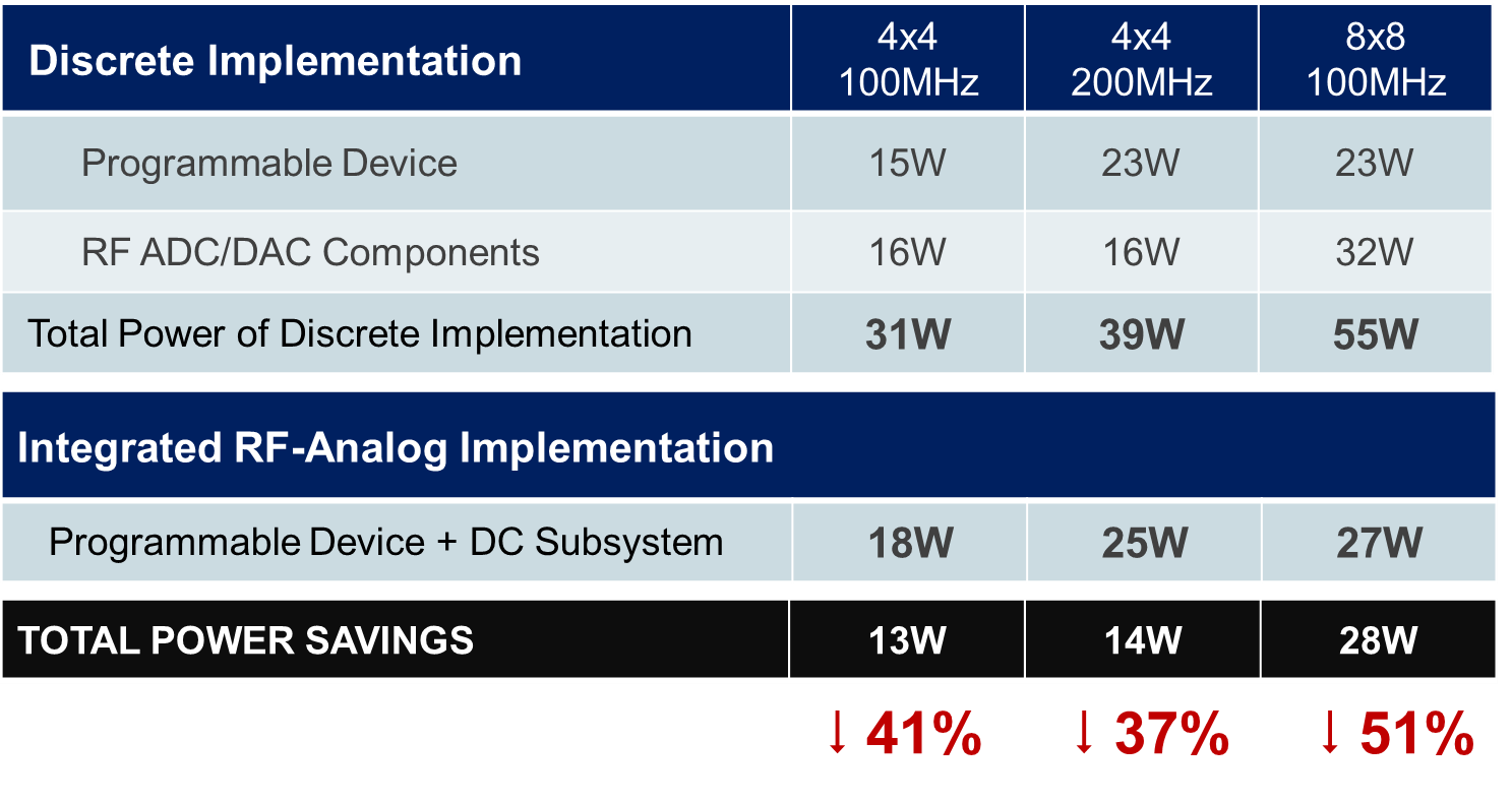
Providing this tightly integrated solution not only reduces the required board area but also reduces the overall power dissipation. As power scales with the sampling frequency, the power reductions provided by a tightly integrated solution become apparent. Figure 3 below identifies the power dissipations for a 4 transmit and 4 Receive system at 100MHz and 200MHz when implemented in both discrete form and within a RFSoC. This power saving becomes even more significant if scaled to an 8 transmit and receive solution.
However, it is not just board area and power where we benefit with the RFSoC concept. Such a tightly coupled device also offers significant reductions in the complexity of sample clock distribution. This provides a simpler clocking scheme, both at the device level and also at the system level as the distribution network is less complex, as much is internal to the device. This simpler clocking network reduces the power and cost associated with distributing GHz clocks on the PCB, offering a more efficient overall solution.
The RFSoC concept, therefore, is capable of providing a more tightly integrated design, which offers the potential for a reduced footprint and power dissipation. What remains is to examine the analogue/RF performance of the ADC and DAC to ensure the required performance can be provided on the traditionally digital CMOS technology.
What Analogue Performance Can We Achieve in Advanced CMOS Technology
Traditionally, high-performance analogue circuits such as ADC and DAC have not used advanced CMOS technology for implementation. However, with digital assistance, it is possible to implement high-performance converters using 16nm CMOS FinFET technology. This is the key that enables the RFSoC concept to be implemented (et al., 2017) (Christophe Erdmann et al., 2017). While the cited works present test chips and do not define the final performance of the RFSoC device, these initial test results warrant further discussion.
Two test chips were developed to examine the potential RF/Analog performance in such a technology. The first implemented an ADC and digital circuitry, while the second implemented a DAC convertor and its digital circuitry. The ADC test chip implemented a three-stage asynchronous pipelined SAR with open-loop integrator-based amplifiers as shown in Figure 4.
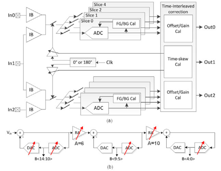
This architecture was selected as it allows maximization of the sampling frequency, resolution and linearity. To ensure reduced power, noise and cost, the architecture is supported by several dynamic circuits and multiple digital calibration loops. The ADC design is configurable to support either dual channel conversion using inputs In0 and In2 (in Figure 4 at 2 GSPS), or a single-channel conversion at 4 GSPS using In1. This approach is what enables the ADC to support either direct RF or I/Q architectures. However, using the 4 GSPS sampling rate provides more flexibility within the frequency planning as it supports a wider bandwidth. Each 2 GSPS ADC slice contains four 500 MSPS ADCs, which operate in an interleaved manner. To address PVT and leakage issues impacting performance at low sampling frequencies, an asynchronous clocking scheme is implemented within the ADC.
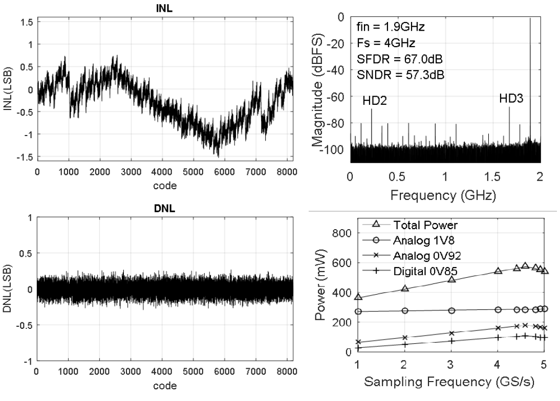
The results obtained for this ADC test chip at 4 GSPS in direct RF mode are INL +/-1.5 LSB and DNL +/-0.3 LSB. While applying an input of -1dBFS signal at 1.9 GHz, the convertor provides a SFDR of 67.0 dB and SNDR of 57.3 dB while total power at 4 GSPS is 513 mW as shown in Figure 5.
The DAC test chip implements a mixing-DAC, which provides full operation across the first, second and third Nyquist zones, that is enabled by implementing mixing within the data path. As with the ADC the DAC test chip, this implements a dual-mode RF DAC with current steering outputs.