Introduction
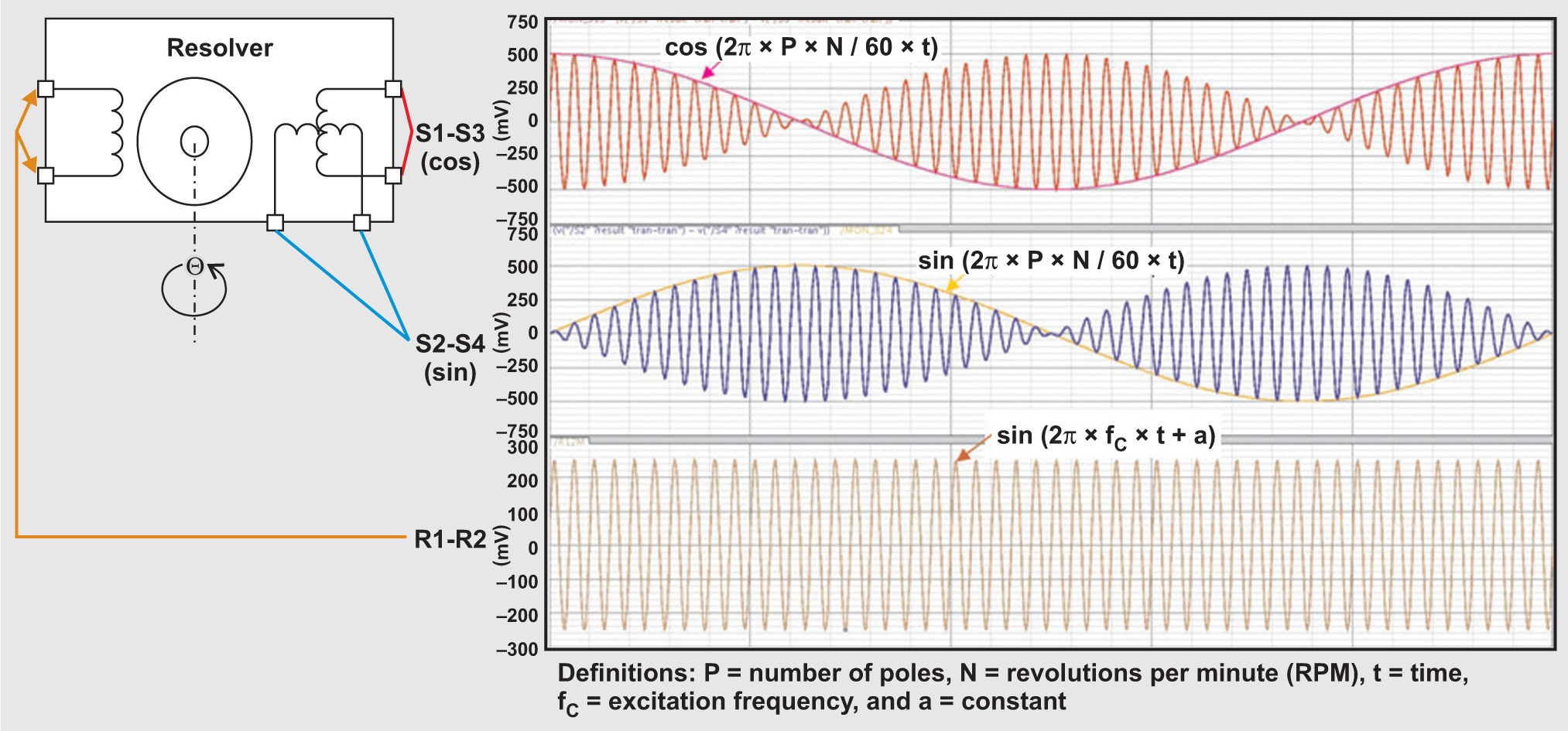
The resolver sensor measures the motor position using a transformer-like action. As shown in Figure 1, a resolver sensor has one rotor winding (R1-R2) with the exciter sine wave that is AC-coupled to two stator windings. The stator windings, a sine coil (S2-S4), and a cosine coil (S1-S3) are mechanically positioned 90 degrees out-of-phase. As the rotor spins, the rotor position angle (Θ) changes with respect to the stator windings. The resulting amplitude modulated signals shown in Figure 1 are typical resolver output signals. These signals must be gained, demodulated and post processed to extract angle and velocity information. There are two ways to do this: one is to use a direct analog-to-digital conversion and another approach is to use comparators and feedback loops.
Direct Analog-to-Digital Conversion
The analog signal from the resolver sensor is passed through an anti-aliasing filter, followed by sampling, and quantization to result into a digital output. The quantization process creates finite number of input steps and finite number of quantization levels that result into quantization error. For example, for a 3-bit quantizer, the distinct output codes at the output are 2^3 = 8 distinct output codes. The digital output is bounded within a certain step range. The quantization process adds “noise” to the samples. This noise power has a distribution over frequency that affects the signal-to-noise ratio (SNR).
SNR is typically given by 6.02B + 1.76 dB
B (number of bits) = 8, SNR is 50 dB, B = 12, SNR is 74 dB, B = 16, SNR is 98 dB, B = 20, SNR is 122 dB
The quantization noise power has a specific distribution over frequency. The harmonics may cause issues if they fall into the excitation frequency band of the resolver-to-digital conversion.
Oversampling ADCs
The sampling theorem needs the sampling frequency to be at least twice the maximum signal frequency of the analog signal. With oversampling or sampling faster, the design of the anti-aliasing filter at the input becomes easier or lower order. The oversampling affects the noise spectrum as well.
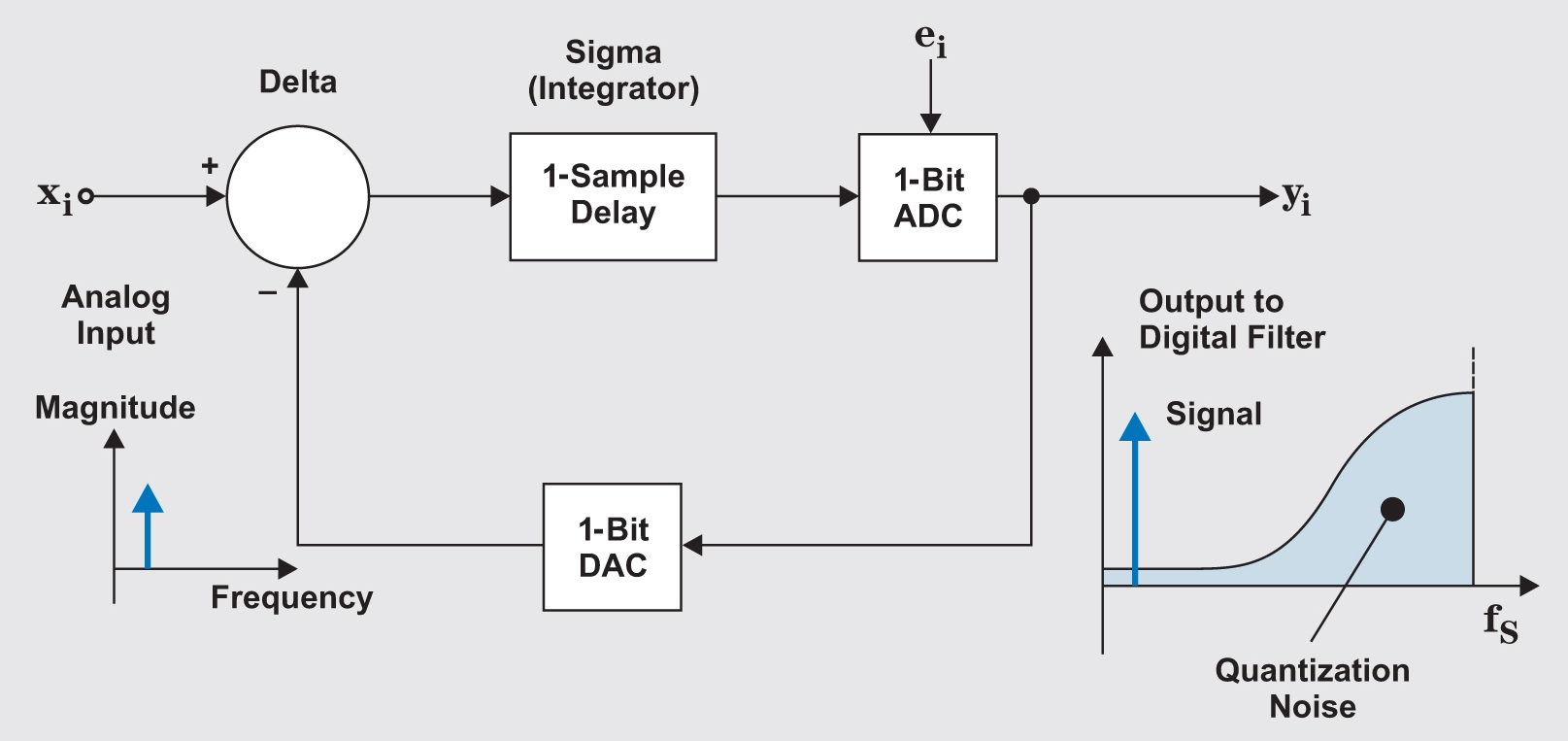
If we are to assume that the quantization error sequence is random in nature, the noise introduced by the quantization process is evenly distributed across all frequencies. So, if we follow the quantization process with a digital low-pass filter with a cut off of the maximum signal frequency, the totally quantization noise at the digital output is proportional to the oversampling ratio. Thus, the design of the analog-to-digital converter (ADC) becomes a critical element in deciding how the quantization noise shaped at frequencies of interest such as the feedback techniques in the analog-to-digital conversion helps achieve this function. The frequency spectrum for oversampling ADC architecture used for resolver-to-digital converter looks like in Figure 2.
Alternative Architecture
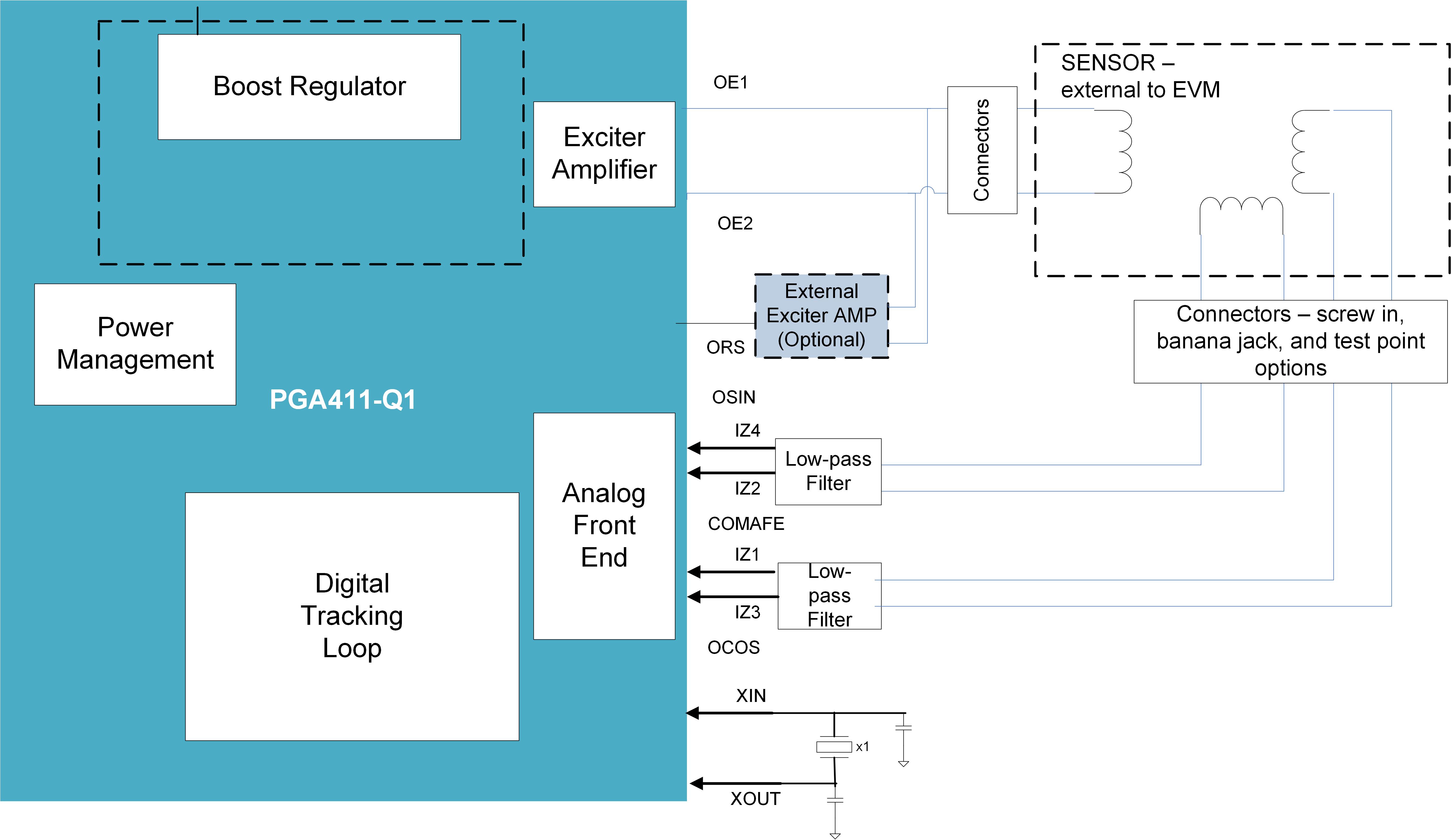
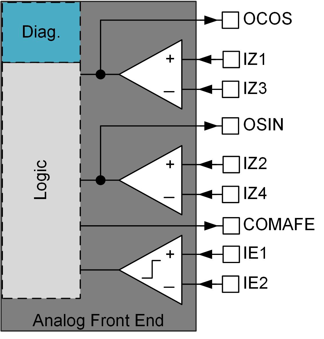
We learned earlier about a technique that has an analog front-end architecture implemented with a delta sigma oversampling ADC that directly samples sine and cosine signals. In this section, the alternative architecture, as shown in Figure 3 and Figure 4, is designed with input comparators implemented in the analog front-end (AFE). The comparators help reject any common-mode noise in the system. The AFE consists of programmable gain amplifiers and a comparator. The AFE block conditions the resolver’s output signals by removing noise, sets the correct input DC bias, and appropriately gains up the AC signal to be used by the subsequent blocks.
A digital feedback loop is the main part of the resolver-to-digital converter (RDC) implementation. It starts by assuming a digital angle, phi. This angle is digitally processed using the sine and cosine lookup tables stored in its memory. This in turn is fed to the corresponding sine and cosine digital-to-analog converters (DACs). The DAC outputs are multiplied with the amplitude-modulated resolver signals (Equations 1 and 2), which are the sine and cosine inputs to the RDC.
Resolver sensor sine signal = sin Θ × sin ωt (1)
Resolver sensor cosine signal = cos Θ × sin ωt (2) where Θ = resolver shaft angle and ω = excitation frequency applied at R1-R2.
The main objective of the RDC architecture is to calculate the rotation angle (Θ) and the velocity of the resolver shaft.
Another key capability that we can achieve with this architecture, besides the advantage of using comparators at the input to reject any common-mode noise and to avoid the oversampling noise effects of the delta sigma ADC architecture, is the AFE automatic offset correction feature. The AFE helps to correct the offset drift of the AFE components, such as input amplifiers in the signal-conditioning stage.
On the system level, AFE offset correction helps to maintain accurate control of the motor control algorithm, irrespective of changes in temperature. The sine and cosine output signals coming from the resolver are relatively small in magnitude, and the amplifier offset drift with temperature and so on must be measured and removed from the AFE amplifiers to ensure correct operation. The offset process occurs on every device power-up when the device enters diagnostics state and then every 100 ms while the device is operating in the normal state. Note that during the time-period for automatic offset correction (around 200-400 µs), the output of an AFE, such as the PGA411-Q1 device, is held at the last good value before the procedure began.
The temperature inside the car/industrial environment, especially where the motor control printed circuit board (PCB) is kept, can tend to increase quickly; hence, it is important to correct for the offset. This feature is implemented by shorting the inputs together and passing the signal through a comparator that goes into a digital circuit correcting the offset calibration.
With an input front-end architecture implemented with the delta sigma ADC that directly sample sine and cosine signals, offset calibration is hard to implement. The alternative architecture shown in Figure 4 is designed to take system operation in a noisy environment into consideration in order to mitigate the common-mode noise, which is a big concern for automotive and industrial applications.
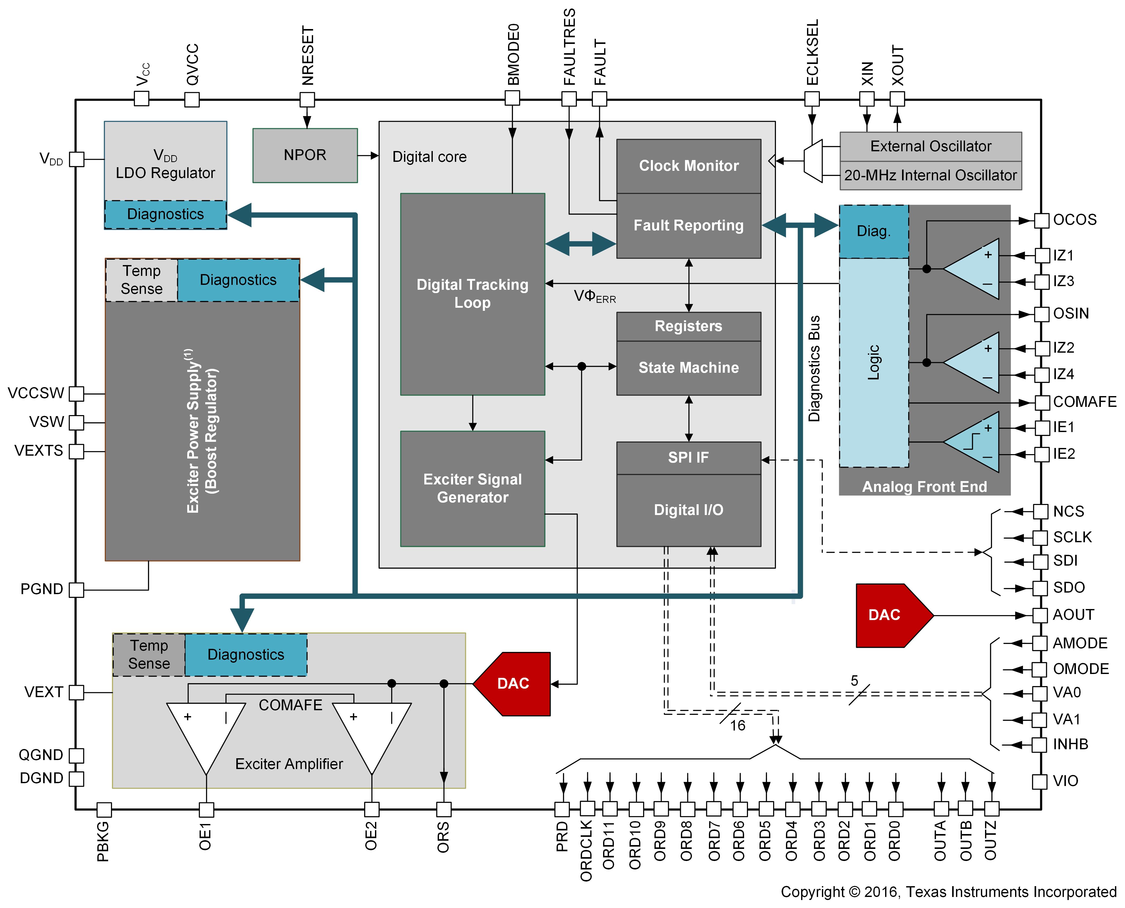
The AFE offset calibration implemented in Figure 5 helps to improve system accuracy because the calibration circuit can correct for any offset drifts resulting from temperature and noise that couples from the insulated-gate bipolar transistor (IGBT) motor driver running in the same enclosure as the resolver control board. This is a common concern of automotive and industrial customers; hence, the purpose of the AFE offset calibration.
In the final application, during those 200-400 µs, the output will be kept at the last known previous state while the system is automatically corrected for offset. In the motor control board, microcontroller needs the motor / resolver position information once in every inverter switching cycle – which will depend on the driver switching frequency. The inverter can use the position information from the previous state to control the inverter and the board.
Conclusion
The architecture chosen for the resolver-to-digital converter can have a huge impact on harmonics, noise and system performance, given the resolver signals are small in amplitude (4/7 Vrms with typically a transformation ratio <0.5). An example where this architecture is being implemented is in the PGA411-Q1, an RDC with integrated exciter amplifier and power supply. Hence, make sure you consider all possible ways in which different architectures for implementation of resolver-to-digital converters can impact your system.